Graphene was very first found experimentally in 2004, bringing intend to the development of high-performance electronic gadgets. Graphene is a two-dimensional crystal composed of a solitary layer of carbon atoms organized in a honeycomb shape. It has an unique digital band structure and exceptional electronic homes. The electrons in graphene are massless Dirac fermions, which can shuttle at exceptionally fast speeds. The service provider flexibility of graphene can be greater than 100 times that of silicon. “Carbon-based nanoelectronics” based on graphene is anticipated to usher in a brand-new era of human information society.

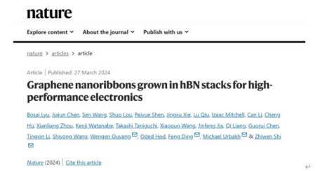
(Graphene nanoribbons grown in hBN stacks for high-performance electronics on “Nature”)
Nonetheless, two-dimensional graphene has no band space and can not be straight made use of to make transistor tools.
Academic physicists have actually proposed that band voids can be introduced with quantum confinement effects by reducing two-dimensional graphene into quasi-one-dimensional nanostrips. The band space of graphene nanoribbons is inversely symmetrical to its size. Graphene nanoribbons with a width of less than 5 nanometers have a band gap comparable to silicon and appropriate for manufacturing transistors. This type of graphene nanoribbon with both band space and ultra-high flexibility is among the ideal prospects for carbon-based nanoelectronics.
Because of this, clinical researchers have spent a lot of energy in studying the prep work of graphene nanoribbons. Although a range of techniques for preparing graphene nanoribbons have actually been established, the problem of preparing top quality graphene nanoribbons that can be used in semiconductor devices has yet to be addressed. The provider movement of the prepared graphene nanoribbons is much lower than the theoretical worths. On the one hand, this distinction originates from the low quality of the graphene nanoribbons themselves; on the various other hand, it comes from the disorder of the atmosphere around the nanoribbons. As a result of the low-dimensional properties of the graphene nanoribbons, all its electrons are revealed to the external setting. For this reason, the electron’s motion is incredibly conveniently impacted by the surrounding environment.
(Concept diagram of carbon-based chip based on encapsulated graphene nanoribbons)
In order to boost the efficiency of graphene devices, lots of techniques have actually been attempted to minimize the condition results brought on by the setting. One of the most successful approach to date is the hexagonal boron nitride (hBN, hereafter referred to as boron nitride) encapsulation method. Boron nitride is a wide-bandgap two-dimensional layered insulator with a honeycomb-like hexagonal lattice-like graphene. Much more notably, boron nitride has an atomically flat surface and outstanding chemical security. If graphene is sandwiched (enveloped) between two layers of boron nitride crystals to create a sandwich framework, the graphene “sandwich” will certainly be separated from “water, oxygen, and microbes” in the complicated exterior setting, making the “sandwich” Always in the “best quality and best” condition. Multiple research studies have actually revealed that after graphene is enveloped with boron nitride, many properties, consisting of service provider movement, will be significantly improved. However, the existing mechanical packaging techniques can be extra efficient. They can currently just be utilized in the field of clinical research study, making it challenging to fulfill the requirements of large-scale manufacturing in the future innovative microelectronics market.
In reaction to the above difficulties, the team of Professor Shi Zhiwen of Shanghai Jiao Tong College took a new strategy. It created a new prep work method to attain the embedded growth of graphene nanoribbons in between boron nitride layers, forming a special “in-situ encapsulation” semiconductor residential property. Graphene nanoribbons.
The growth of interlayer graphene nanoribbons is attained by nanoparticle-catalyzed chemical vapor deposition (CVD). “In 2022, we reported ultra-long graphene nanoribbons with nanoribbon sizes approximately 10 microns expanded externally of boron nitride, yet the length of interlayer nanoribbons has far surpassed this record. Currently limiting graphene nanoribbons The upper limit of the size is no longer the growth system yet the size of the boron nitride crystal.” Dr. Lu Bosai, the initial writer of the paper, stated that the size of graphene nanoribbons grown between layers can get to the sub-millimeter level, far exceeding what has actually been formerly reported. Outcome.
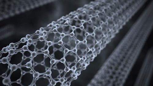
(Graphene)
“This sort of interlayer embedded growth is remarkable.” Shi Zhiwen stated that product development usually includes growing one more on the surface of one base product, while the nanoribbons prepared by his study team grow directly externally of hexagonal nitride in between boron atoms.
The aforementioned joint research study group functioned very closely to reveal the growth device and found that the development of ultra-long zigzag nanoribbons between layers is the outcome of the super-lubricating properties (near-zero rubbing loss) in between boron nitride layers.
Speculative monitorings reveal that the growth of graphene nanoribbons just takes place at the particles of the catalyst, and the placement of the stimulant stays the same throughout the procedure. This reveals that the end of the nanoribbon puts in a pushing pressure on the graphene nanoribbon, causing the whole nanoribbon to overcome the friction in between it and the bordering boron nitride and constantly slide, causing the head end to move away from the stimulant fragments gradually. Consequently, the researchers guess that the rubbing the graphene nanoribbons experience must be very small as they move between layers of boron nitride atoms.
Since the grown up graphene nanoribbons are “enveloped sitting” by shielding boron nitride and are shielded from adsorption, oxidation, environmental air pollution, and photoresist contact during device processing, ultra-high performance nanoribbon electronic devices can theoretically be gotten gadget. The scientists prepared field-effect transistor (FET) devices based on interlayer-grown nanoribbons. The measurement results revealed that graphene nanoribbon FETs all exhibited the electrical transport qualities of typical semiconductor devices. What is even more noteworthy is that the gadget has a provider mobility of 4,600 cm2V– ones– 1, which goes beyond previously reported outcomes.
These superior properties indicate that interlayer graphene nanoribbons are expected to play a vital function in future high-performance carbon-based nanoelectronic gadgets. The study takes a vital action towards the atomic construction of innovative packaging styles in microelectronics and is anticipated to influence the field of carbon-based nanoelectronics substantially.
Supplier
Graphite-crop corporate HQ, founded on October 17, 2008, is a high-tech enterprise committed to the research and development, production, processing, sales and technical services of lithium ion battery anode materials. After more than 10 years of development, the company has gradually developed into a diversified product structure with natural graphite, artificial graphite, composite graphite, intermediate phase and other negative materials (silicon carbon materials, etc.). The products are widely used in high-end lithium ion digital, power and energy storage batteries.If you are looking for first graphene, click on the needed products and send us an inquiry: sales@graphite-corp.com
Inquiry us